Introduction
NAND flash memory is a common form of storage media, with wide applications from small form factor mobile devices to datacenter storage. However, as modern flash cells are continuously slimmed down in size, the read disturbance problem is becoming one of the main factors accounting for the reliability issues found with NAND flash memories. A read disturbance problem, in short, occurs after a large amount of read tasks are performed to pages within the same block, causing the digital values of cells nearby the cells being read to change, and thus inducing data errors.
How does read disturbance happen?
Every NAND flash memory cell has a floating gate transistor with a control gate connected to the word-line, and a source and a drain connected to its neighboring cells on the same bit-line. The floating gate transistor is situated beneath the control gate. The amount of electrons stored in the floating gate determines the threshold voltage of the transistor.
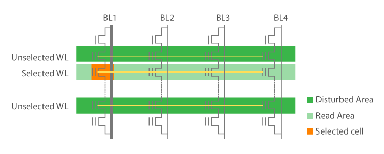
To find out if there are any electrons trapped on a particular floating gate, the memory device must read the entire word. In order to read the cells in a selected row (shown in light green), a higher voltage must be applied to its neighboring unselected word-lines (shown in deep green) in the same block. In the meantime, one selected cell will be read per bit-line for the device to determine its digital value, i.e. whether it stores a 0 or a 1. The high voltage applied on the neighboring transistor gates attracts electrons to the floating gate, slightly raising the cell threshold voltage with each read, and “disturbing” the cells in the process. Over time, the threshold voltage of a cell in an “un-programmed” state, which means that it stores a 1, increases and accumulates enough to eventually shift to a “programmed” state, which means that it stores a 0. This is known as the Read Disturbance phenomenon. The change of state is an irreversible process, and once changed, the bit value will not “flip” back unless the block is otherwise erased.
Transcend’s solutions
Read disturbance can be reduced by minimizing excessive reads. Transcend offers three different solutions to address this problem.
-
Wear leveling algorithm: This feature spreads the NAND flash memory cell usage over the available memory array, making sure that the data are equally written within the block.
- Early move: This feature detects and corrects potential data errors. If error bits in a block reach upper limit, then the data should be moved to another block and the original block should be erased. (Note: Some products do not have this feature.)
-
Read retry: This feature is designed for flash memory to adjust the read reference voltage and eliminate the read error.